JFET
Aim
- To measure drain current (𝐼𝑑) at different values of gate voltage.
- To measure drain current (𝐼𝑑) for different values of drain–source voltage. To plot input/output characteristics curves and evaluate the parameters.
Apparatus
- JFET (BFW10)
- Breadboard
- Regulated Power Supply (0 – 2 V) and (0 – 12 V)
- Ammeters (0 – 20 mA)
- Voltmeter V₁ (0 – 2V)
- Voltmeter V₂ (0 – 10V)
- Connecting Wires (Single Strand)
Theory
A Junction Field-Effect Transistor (JFET) is a three-terminal semiconductor device used for amplification or switching electronic signals. Its operation is based on the control of current flow between two of its terminals (the source and the drain) by a voltage applied to the third terminal (the gate).
The drain current (𝐼𝑑) of the JFET is controlled by the application of reverse-biased voltage between gate and source terminals (𝑉𝐺𝑆). The relationship between 𝐼𝑑 and 𝑉𝐺𝑆 is defined by the well-known Shockley’s equation.
$$I_d = I_{dss} \left(1 - \left(\frac{V_{gs}}{V_p}\right)^2\right)$$
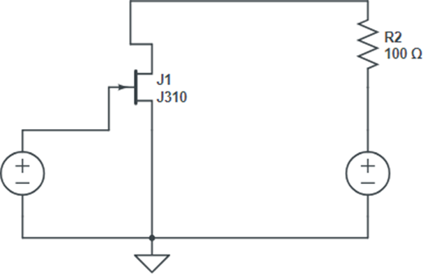
Circuit Diagram
Procedure
Drain Characteristics
- Connect the circuit as shown in Figure 1.
- Keep 𝑉𝐺𝑆 = 0V by varying 𝑉𝐺𝐺.
- Gradually vary 𝑉𝐷𝐷 in steps of 1V up to 10V and note down the drain current 𝐼𝑑 and the drain-to-source voltage (𝑉𝐷𝑆).
- Repeat the above procedure for 𝑉𝐺𝑆 = -0.4V, -0.8V, -1.2V, and -1.6V.
- Plot the drain characteristics by taking 𝑉𝐷𝑆 on the X-axis and 𝐼𝑑 on the Y-axis for a constant 𝑉𝐺𝑆.
Transfer Characteristics
- Connect the circuit as shown in Figure 1.
- Set 𝑉𝐷𝑆 = 4V/8V.
- Gradually vary 𝑉𝐷𝑆 in steps of 0.5V until the current 𝐼𝑑 reduces to a minimum value.
- Gradually vary 𝑉𝐺𝐺 and note down both the drain current 𝐼𝑑 and the gate-source voltage (𝑉𝐺𝑆).
- Repeat the above procedure for 𝑉𝐷𝑆 = 4V/8V.
- Plot the transfer characteristics by taking 𝑉𝐺𝑆 on the X-axis and 𝐼𝑑 on the Y-axis at constant 𝑉𝐷𝑆.
Observations
Drain characteristics
| S. No. | 𝑉𝐺𝑆= 0 | 𝑉𝐺𝑆= -0.4 | 𝑉𝐺𝑆= -0.8 | 𝑉𝐺𝑆= -1.2 | 𝑉𝐺𝑆= -1.6 | |||||
|---|---|---|---|---|---|---|---|---|---|---|
| 𝑉𝐷𝑆 | 𝐼𝑑 | 𝑉𝐷𝑆 | 𝐼𝑑 | 𝑉𝐷𝑆 | 𝐼𝑑 | 𝑉𝐷𝑆 | 𝐼𝑑 | 𝑉𝐷𝑆 | 𝐼𝑑 | |
| 1 | ||||||||||
| 2 | ||||||||||
| 3 | ||||||||||
Transfer characteristics
| s.no. | 𝑉𝐷𝑆 = 4V | 𝑉𝐷𝑆= 8V | ||
|---|---|---|---|---|
| 𝑉𝐺𝑆 | 𝐼𝑑 | 𝑉𝐺𝑆 | 𝐼𝑑 | |
| 1 | ||||
| 2 | ||||
| 3 | ||||
Precautions
- Avoid double connections if possible.
- Ensure all connections are proper and tight.
Result
The drain and transfer characteristics of the FET were studied successfully.